
High-Quality Wafer Technology in Solar Panels for Enhanced Efficiency
By:Admin
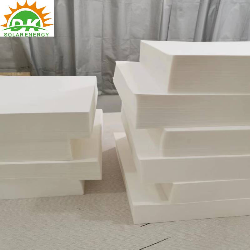
In the rapidly evolving landscape of renewable energy, solar technology continues to make significant strides, thanks to continual advancements in material science and manufacturing processes. One of the critical components driving improvements in solar panel performance is the wafer—the thin slice of semiconductor material that serves as the foundational element in photovoltaic (PV) cells. Recent developments in wafer technology have demonstrated promising potential to enhance the efficiency, durability, and cost-effectiveness of solar panels, thereby accelerating the global transition toward sustainable energy.
### Understanding the Importance of Wafers in Solar Panels
A solar panel comprises numerous photovoltaic cells, each typically made from crystalline silicon wafers. These wafers are meticulously processed to convert sunlight into electric current, forming the backbone of solar power generation. The quality, thickness, and size of wafers significantly influence the overall efficiency of solar cells. Innovations in wafer design, including the use of larger diameters, thinner substrates, and improved crystal structures, are pivotal in maximizing light absorption and charge carrier mobility.
For instance, the shift from traditional 156mm wafers to larger 182mm or even 210mm wafers has allowed manufacturers to increase the active surface area of each cell, thereby capturing more sunlight without proportionally increasing the cost of production. Additionally, thinner wafers reduce raw material consumption and lower manufacturing expenses, although they require advanced handling technologies to maintain structural integrity.
### Recent Innovations Driving Solar Panel Advancements
The solar industry has seen several notable advancements related to wafer technology. High-purity monocrystalline silicon wafers now dominate the market due to their superior electrical properties. Innovations such as diamond wire sawing have minimized kerf loss during wafer slicing, increasing yield from silicon ingots and reducing waste. Surface passivation techniques and texturing processes have also improved, enabling wafers to receive and convert more sunlight with less reflection.
Another trend is the adoption of heterojunction technology (HJT), where traditional silicon wafers are combined with thin amorphous silicon layers to create cells with significantly higher efficiencies and better temperature coefficients. This combination enhances the wafer’s ability to convert sunlight into electricity, even under less-than-ideal weather conditions.
Moreover, manufacturers are exploring bifacial wafer designs, allowing solar panels to capture sunlight from both the front and rear sides. This approach increases power output by utilizing reflected and diffused light, especially in installations with reflective ground surfaces or strategic panel layouts.
### Environmental and Economic Impacts
Manufacturing efforts focusing on wafer technology improvements also aim to reduce the environmental footprint of solar panel production. By optimizing wafer thickness and reducing material consumption, manufacturers lower the embodied energy of each panel. These changes contribute to a shorter energy payback time—the period required for the panel to generate the amount of energy consumed during its manufacture.
Economically, wafer innovations facilitate cost reductions in terms of raw materials and production processes, making solar power more accessible and competitive with fossil fuels. The scalability of wafer production technologies allows for mass manufacturing without sacrificing quality, supporting global demand as countries ramp up renewables to meet climate goals.
### Company Introduction: Driving Innovation in Solar Wafer Technology
At the forefront of these developments is a leading solar technology company (company name not disclosed). Established with a commitment to innovation and sustainability, the company has consistently pioneered advanced wafer manufacturing techniques that set industry standards. Their research and development center focuses on producing high-quality crystalline silicon wafers tailored to optimize the latest photovoltaic cell architectures.
The company's vertical integration strategy covers the entire production chain—from silicon ingot growth to wafer slicing and final cell processing—ensuring strict quality control and process efficiency. State-of-the-art equipment and automated handling systems minimize defects and increase throughput, enabling the company to supply wafers that meet the stringent performance requirements of top-tier solar panel manufacturers worldwide.
Beyond technological excellence, the company emphasizes environmental responsibility, employing green manufacturing practices that reduce chemical usage, waste generation, and energy consumption. Their commitment to sustainable development aligns with global efforts to combat climate change and promote renewable energy adoption.
### Looking Ahead: The Future of Wafer Technology in Solar Energy
As the global demand for renewable energy escalates, wafer innovation remains a central pillar in the advancement of solar power technologies. Future developments may include the integration of novel materials such as perovskites with silicon wafers to create tandem cells with efficiencies surpassing current limits. Additionally, improvements in wafer robustness and flexibility can expand solar applications into new domains, including building-integrated photovoltaics and portable solar devices.
Collaborations between material scientists, engineers, and solar manufacturers will be critical in overcoming the technical challenges of wafer production while driving down costs. The continued refinement of wafer technologies promises not only to boost solar panel efficiency but also to make solar energy more affordable and accessible worldwide.
### Conclusion
Wafer technology plays a vital role in shaping the future of solar energy, enabling panels to capture more sunlight and convert it into clean electricity more efficiently and sustainably. Through advanced manufacturing processes and innovative material use, the solar industry is poised to deliver solutions that meet the world's growing energy needs while safeguarding the environment. Companies leading this innovation path are crucial partners in achieving a sustainable energy future, proving that even the thinnest slice of silicon can have a massive impact on global clean energy generation.